Register Settings of RT9467 when its Parallel Charging with Switching Capacitor
AN080
In portable device applications, designers usually parallel switching capacitor chargers with a switching charger to enhance charging efficiency and reduce charging time. This application note provides the register control settings of the RT9467 when the system transitions from battery charging with a switching charger to using switching capacitor chargers. Note that users must follow this application note for the charging process.
1 Charging System Structure
Figure 1 presents a simplified block diagram of the charging system. In this charge system, a smart capacitor divider charger is used to detect the USB BC1.2 standard of the adapter, and the PD controller is used to communicate with the adapter by the PD protocol. Once the smart wall adapter is detected, the AP will control both the switching charger and smart capacitor divider charger to achieve a high current charging period. These devices can communicate with the AP through an I2C serial interface.
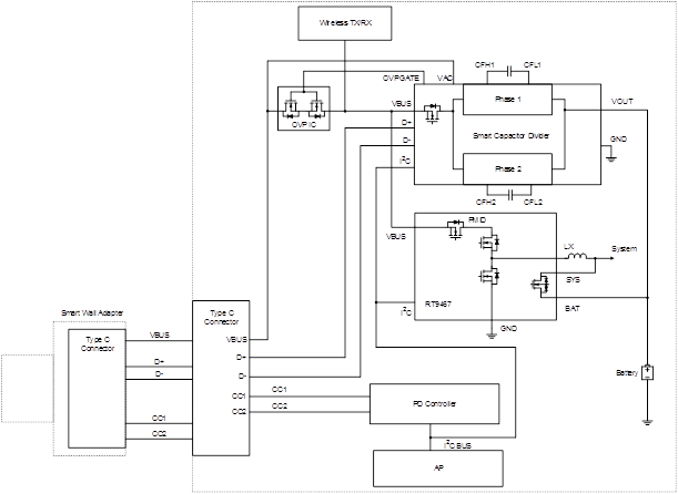
Figure 1. Function Block Diagram of the Charging System
The charge profile of a high-capacity battery using the RT9467 and a capacitor divider charger is shown in Figure 2. In order to achieve the charge profile, the RT9467 is required to dominate the pre-charge, fast charge when the battery voltage is lower than the system startup voltage, constant voltage, and termination periods, respectively. The capacitor divider charger is used to achieve the fast charge period. To shorten the constant voltage period, the capacitor divider charger is controlled to reduce the charge current by ramp steps.
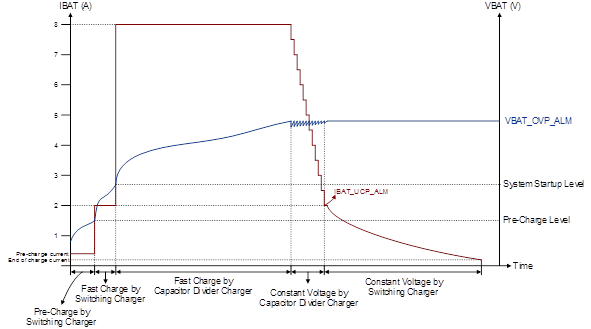
Figure 2. Charge Profile Using the RT9467 and Smart Capacitor Divider Charger
2 RT9467 Software Notice
When the RT9467 starts up, it sets the system voltage before the capacitor divider charger enters the fast charge period. Especially, setting the RT9467 MIVR to 13.4V causes the RT9467 to stop switching, as shown in Figure 4. In this moment, only Q1 and Q2 are turned off, while QRB remains on, as shown in Figure 3. Therefore, when VBUS is plugged out in the fast charge period by the capacitor divider charger, both VBUS and PMID discharge at the same time to prevent VDS from exceeding the clamping voltage of the QRB MOS when VBUS voltage changes drastically. After VBUS is plugged out, VBUS is lower than the VBUS_INSERT of the smart capacitor divider charger. Set the RT9467 MIVR to 4.4V (default) and wait for VBUS to be plugged in again.
The host must set the RT9467 registers step by step. The programming steps are shown as below:
1. Write REG0x06 = 0xFF (after the system wakes up, set MIVR to 13.4V)
2. Write REG0x06 = 0x0B (when VBUS < VBUS_INSERT, set MIVR to 4.4V (default))
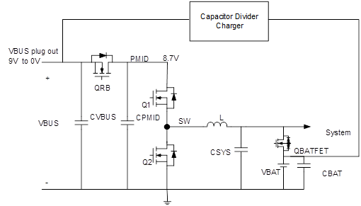
Figure 3. Circuit Diagram of RT9467
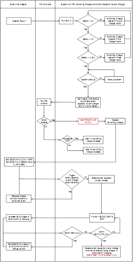
Figure 4. System Control Flow Chart
3 Conclusion
In conclusion, the information provided in this application note includes the necessary settings when the RT9467 in parallel with a switching capacitor. By setting the MIVR voltage higher than the VBUS voltage when the system is charging with the switching capacitor, the RT9467 will turn on QRB (the MOS between VMID and VBUS) and stop switching. This setting meets the requirements of fast charging systems and prevents the VMID-VBUS voltage from exceeding the QRB's AMR when the system is charging with the switching capacitor.
The above summary concludes the contents covered in this application note. To stay informed with more information about our products, please subscribe to our newsletter.
4 Appendix
Functional Register Description
I2C Slave Address: 1011011(5BH)
R/W: Read and write
RWC: Read and write, also automatically cleared by particular conditions
Register Address: 0x06, Register Name: CHG_CTRL6
|
Name
|
Function
|
Addr
|
Reset
|
|
CHG_CTRL6
|
Control 6
|
0x06
|
0x0B
|
|
Bit
|
Mode
|
Name
|
Reset Value
|
Description
|
|
[7:1]
|
R/W
|
VMIVR[6:0]
|
0000101
|
Input MIVR threshold setting
0000000: 3.9V
0000001: 4V
0000010: 4.1V
0000011: 4.2V
0000100: 4.3V
0000101: 4.4V (default)
0000110: 4.5V
…
0011110: 6.9V
0011111: 7V
…
0110010: 8.9V
0110011: 9V
…
1010000: 11.9V
1010001: 12V
…
1011111: 13.4V
1100000 to 1111111: 13.4V
|